HieFo Introduces High Efficiency CW Lasers for Silicon Photonics Transceivers
ALHAMBRA, Calif., March 31, 2025 (GLOBE NEWSWIRE) -- HieFo announced today the product launch of multiple new high-efficiency Continuous Wave DFB indium phosphide (InP) lasers, designed to address the ever-increasing demands of silicon photonics based optical transceivers.
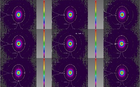
Representative Far Field Pattern (typical 15° X 18°)
Proprietary new design for uncooled intensity modulated direct detect applications
HieFo’s uncooled O-band CW laser family supports the CWDM4 wavelength plan over an operating temperature of -5 to 75°C, while maintaining 70mW minimum optical output power. These performance parameters are achieved using an Aluminum-free active quantum well design, which offers the optical transceiver industry a new standard in terms of proven field reliability and performance, for high operating temperature non-hermetic applications.
New efficiency milestones for Coherent Optical transmission
HieFo has achieved new performance levels with the latest innovations on the previously released HCL30 CW DFB laser chip. Using innovations from 12 recently filed patents, HieFo’s 1mm cavity length laser chip can produce above 200mW typical optical output power while achieving sub 300kHz spectral linewidth performance, all while achieving WPE of 30% or greater over a wide power range. HieFo offers custom O-band wavelength variants of this laser design for various coherent applications ranging from Datacenter to PON architecture.
“HieFo’s latest product advances address the stringent performance standards required by the industry’s leading silicon photonic designs,” stated Harry Moore, HieFo’s Chairman & Co-founder. Mr. Harry added, that, “HieFo continues to execute on our core mission, which is to develop and produce the most efficient and reliable InP based chips in the industry.”
Please contact HieFo at info@hiefo.com for more information.
About HieFo
HieFo Corporation is headquartered at 2015 Chestnut St in Alhambra, California 91803. Through a management buyout, HieFo leverages more than four decades of innovative legacy in optoelectronic devices from EMCORE. HieFo now focuses on development and commercialization of high-efficiency photonic devices for optical communication industries and will continue the pursuit of the most innovative and disruptive solutions to serve datacom, telecom, AI connectivity and general sensing industries. For inquiries, please contact info@hiefo.com.
A photo accompanying this announcement is available at https://www.globenewswire.com/NewsRoom/AttachmentNg/667773e6-ea99-4873-8d9e-1cc1b594309b

![]()
Representative Far Field Pattern (typical 15° X 18°)
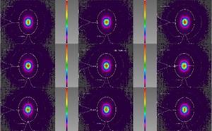
Representative Far Field Pattern (typical 15° X 18°)
Legal Disclaimer:
EIN Presswire provides this news content "as is" without warranty of any kind. We do not accept any responsibility or liability for the accuracy, content, images, videos, licenses, completeness, legality, or reliability of the information contained in this article. If you have any complaints or copyright issues related to this article, kindly contact the author above.
